Device Name Model Picture Main Purpose
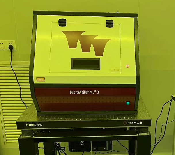
Compact Desktop Maskless Laser Direct Writing Lithography System MicroWriterML3
  • Pattern Transfer from Mask to Substrate
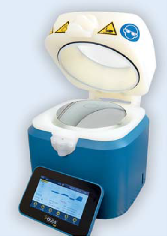
Spin Coater, Hot Plate, and Developer System SPS POLOS
  • Photolithography Ancillary Equipment
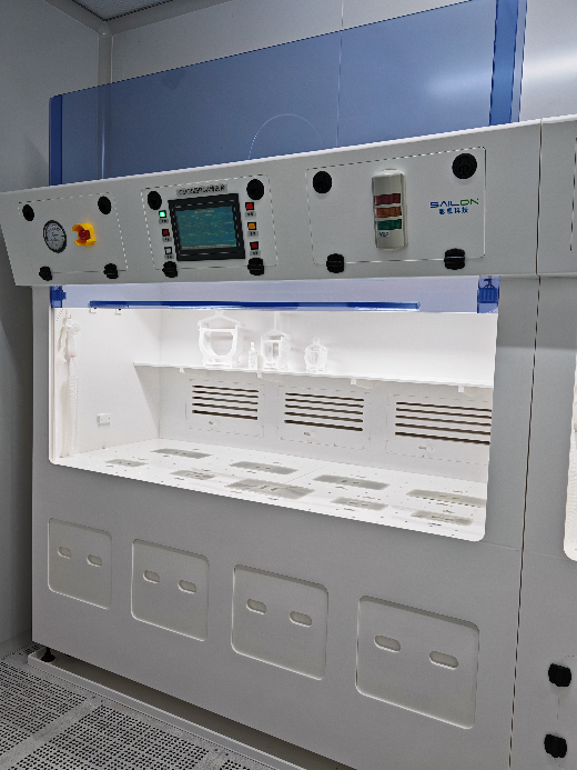
Wet Etching and Cleaning Platform SN-KS200
  • Chemical Etching and Surface Material Removal Using Specialized Reagents
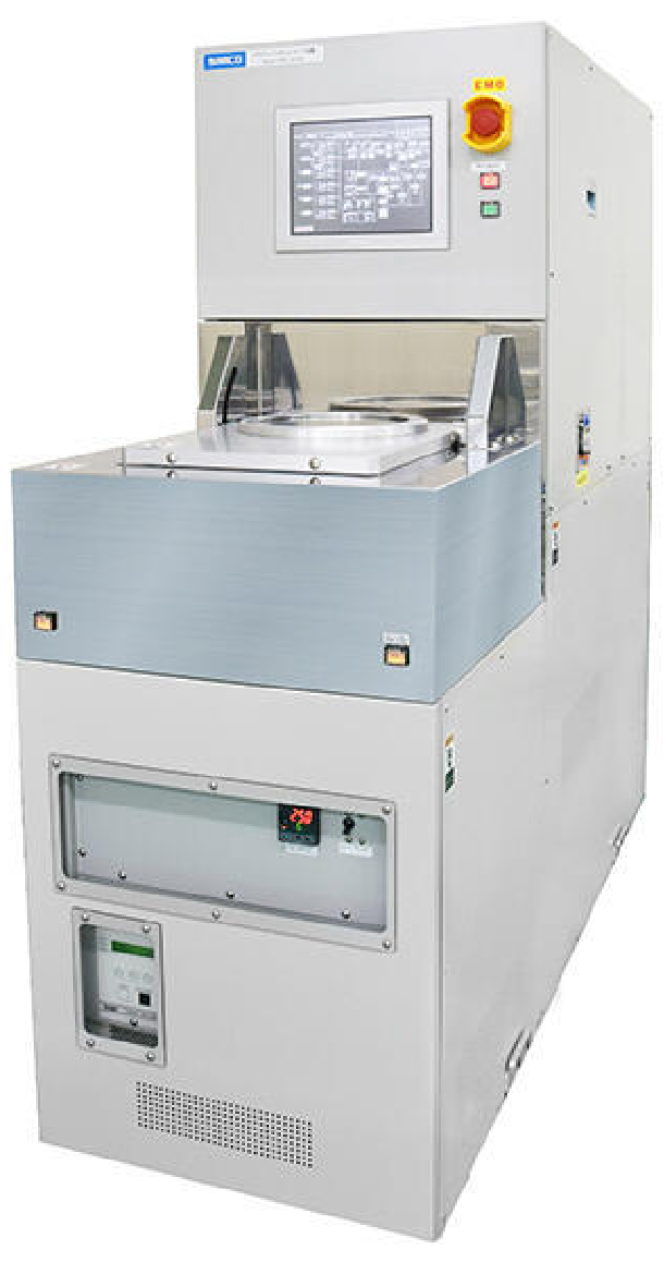
Reactive Ion Etching System SAMCO RIE-200NL
  • The process utilizes gaseous chemical etchants to undergo physical reactions, chemical reactions, or a combination of both physical and chemical reactions with the materials on the silicon wafer that are not covered by photoresist, thereby achieving the removal of exposed surface materials.
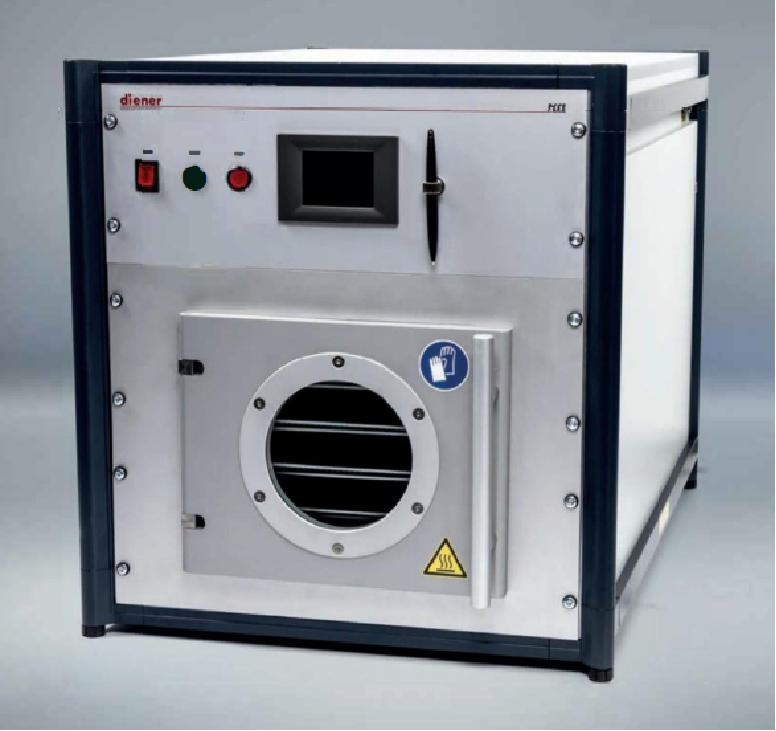
Plasma Cleaning System Nano Low-pressure
  • Surface Plasma Cleaning and Modification Treatment
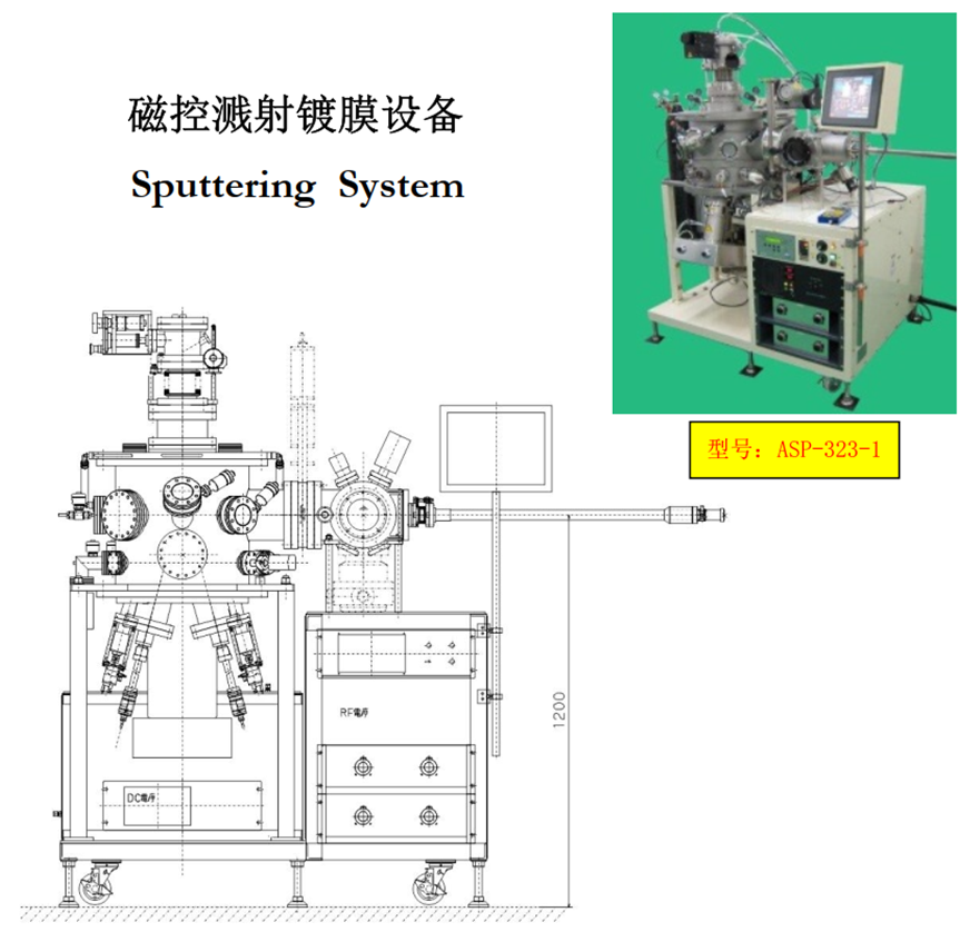
ASP Series Magnetron Sputtering Coating System ANSEI TECH
  • High-Quality Thin Film Deposition
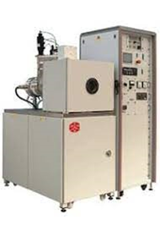
Multi-Target Magnetron Sputtering System HHV-TF600
  • High-Quality Thin Film Deposition
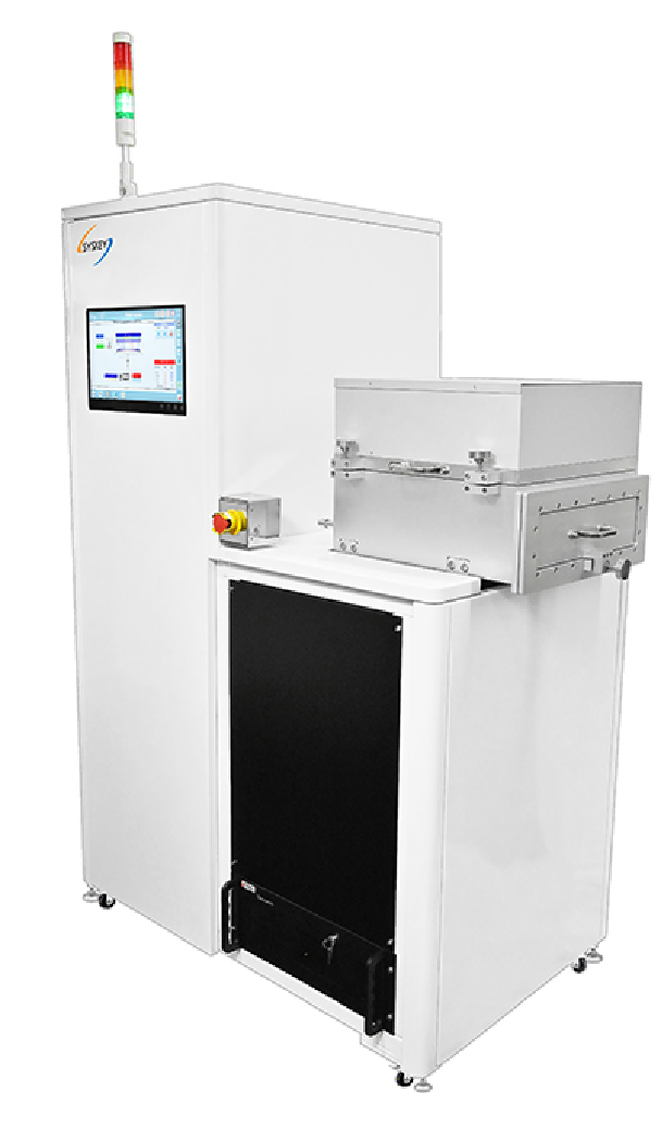
Plasma-Enhanced Atomic Layer Deposition System SC6-PEV
  • High-Quality Thin Film Deposition
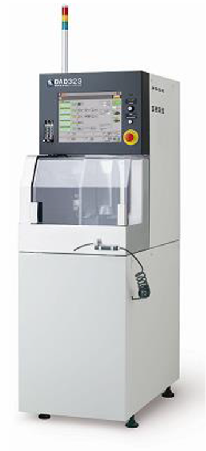
Precision Dicing Saw  
  • The process involves the precise segmentation of the entire wafer with completed circuit fabrication into independent chip units along pre-defined dicing streets.
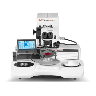
Multi-functional Ball and Wedge Wire Bonder MPP
  • Achieving a tight connection between the bonding wire and the substrate pads.
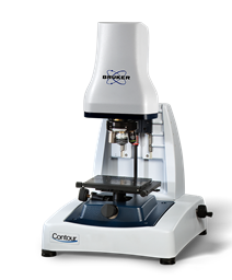
3D Optical Profiler BRUKER ContourX-100
  • Analysis of thin film and device surface morphology
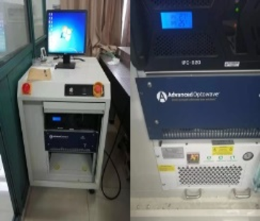
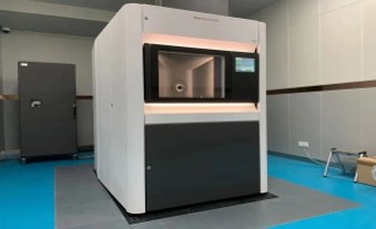
DLP 3D Printer B9 Core 550
波长: 405 nm
  • Rapid prototyping and printing of flexible sensors
Femtosecond Laser Micro-Nano Processing System 600
1032nm 180fs
800 KHz
  • Laser micro-nano processing and metal surface treatment
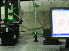
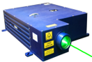
Green Continuous Wave Laser Processing System Verdi G1
532 nm 10 W
  • Laser Direct Writing of Flexible Sensors
  • Laser-Induced Chemical Reactions
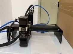
Blue Pulsed Laser 波长:400~450nm
功率:7W
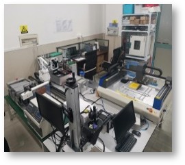
High-precision inkjet printing and hybrid manufacturing platform for flexible circuits and antennas Self-built system
  • Multimodal Intelligent Sensor Manufacturing
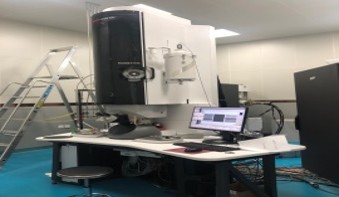
Field Emission Analytical Transmission Electron Microscope FEI Talos F200X
  • Microscopic morphology, crystal structure, and crystal defect analysis of materials
Scanning Electron Microscope-Focused Ion Beam Dual-Beam System FEI Helios G4 UC
  • Three-dimensional material reconstruction, STEM analysis, energy dispersive spectroscopy analysis, and EBSD analysis
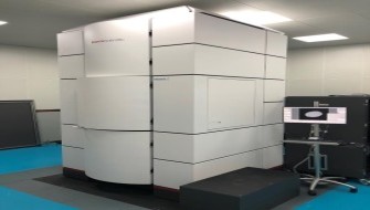
Objective-Corrected Environmental Transmission Electron Microscope FEI Themis ETEM
  • Research on the atomic structure of materials
Double Aberration-Corrected Transmission Electron Microscope FEI Themis Z
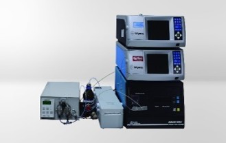
Multi-angle Scattering Instrument Wyatt Dynapro NanoStar
  • Measurement and analysis of molecular weight distribution, root-mean-square radius (radius of gyration), second virial coefficient, and hydrodynamic radius
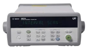
Data Acquisition System Agilent 34972A
  • Data recording and acquisition for sensors and integrated circuits
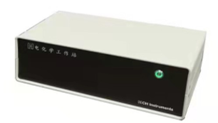
Electrochemical Workstation CHI660E
  • Cyclic voltammetry, electrochemical impedance spectroscopy, and alternating current voltammetry measurements for devices
Impedance Analyzer IM3536
  • Device impedance analysis
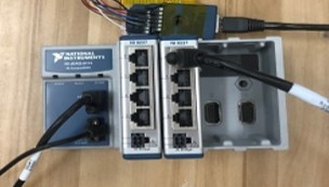
NI Data Acquisition (DAQ) System cDAQ-9174
  • Measurement of sensors, load cells, and bridges
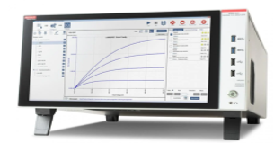
Semiconductor Analyzer Keithley 4200A-SCS
  • Semiconductor characteristic measurement of devices
Vector Network Analyzer 安立MS46322B
  • Testing of passive devices
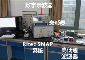
Nonlinear High-Energy Ultrasonic Testing System RAM-5000 SNAP
  • Capable of detecting harmonic frequencies and testing the nonlinear characteristics of materials
  • Equipped with dual gated amplifiers, suitable for nonlinear beam mixing tests involving sum and difference frequency generation
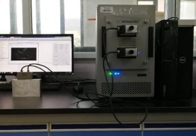
Ultrasonic Testing Platform Vantage 256
  • Up to 256 independent channels for controlling transmission or reception parameters, supporting arbitrary waveform transmission
  • Real-time parameter adjustment to obtain ideal data in a single acquisition
Two-dimensional component two-wave mixing interferometer Tempo
  • Simultaneous detection of out-of-plane and in-plane displacement
  • Ultra-high detection sensitivity
  • Auto-focus functionality